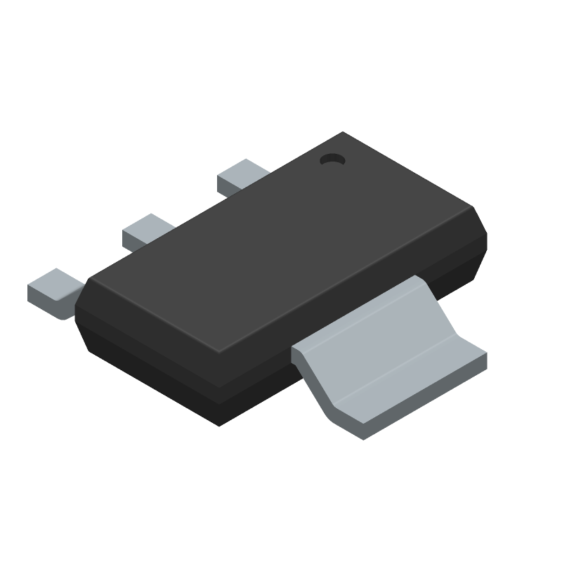
The recommended PCB footprint for the ZXMN10A11GTA is a standard SOT23 package with a 1.3mm x 1.3mm body size. A minimum pad size of 0.8mm x 0.8mm is recommended for reliable soldering.
To ensure proper biasing, connect the input pin (VIN) to a stable voltage source, and the output pin (VOUT) to a load or a voltage divider. The enable pin (EN) should be tied to VIN or a logic signal for proper operation.
The ZXMN10A11GTA is rated for operation from -40°C to 125°C. However, it's recommended to derate the device's performance at extreme temperatures to ensure reliability.
Yes, the ZXMN10A11GTA is AEC-Q100 qualified, making it suitable for automotive and high-reliability applications. However, it's essential to follow the recommended operating conditions and design guidelines to ensure the device meets the required specifications.
To prevent ESD damage, handle the ZXMN10A11GTA with an anti-static wrist strap or mat, and ensure the workspace is ESD-protected. Avoid touching the device's pins or handling it in environments with high electrostatic charges.
 ZXMN10A11GTA datasheet
by Diodes Incorporated
ZXMN10A11GTA datasheet
by Diodes Incorporated