The recommended power-up sequence is to apply VDD (1.2V to 1.4V) first, followed by VIO (1.8V to 3.3V) and then the clock signal. This ensures proper device operation and prevents latch-up.
To optimize the clock tree, use a clock buffer (such as the CDCM6201) to reduce clock skew and jitter. Additionally, ensure that the clock signal is routed close to the device and that the clock tree is balanced to minimize signal degradation.
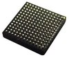
The maximum operating temperature range for the TMS320VC5441GGU is -40°C to 85°C. However, it's recommended to operate the device within the industrial temperature range of -40°C to 70°C for optimal performance and reliability.
A reliable reset circuit can be implemented using a voltage supervisor (such as the TLV7031) that monitors the VDD voltage and asserts a reset signal when the voltage falls below a certain threshold. This ensures that the device is properly reset during power-up and power-down sequences.
To ensure optimal performance and signal integrity, follow these PCB layout guidelines: keep signal traces short and direct, use a solid ground plane, and avoid routing signals under the device. Additionally, use a 4-layer PCB with a dedicated power plane and a dedicated ground plane.
 TMS320VC5441GGU datasheet
by Texas Instruments
TMS320VC5441GGU datasheet
by Texas Instruments