A good PCB layout for the TDA2040V involves keeping the input and output traces as short as possible, using a ground plane, and placing decoupling capacitors close to the IC. A 4-layer PCB with a dedicated ground plane is recommended.
The gain resistor (Rg) value depends on the desired gain and input impedance. A higher Rg value increases the gain, but also increases the noise and distortion. A good starting point is to use the recommended Rg value from the datasheet and adjust it based on your specific application requirements.
The maximum power dissipation of the TDA2040V is 1.4W. However, this value can be affected by the ambient temperature, PCB layout, and thermal management. It's essential to ensure proper heat sinking and thermal design to prevent overheating.
Yes, the TDA2040V can be used as a line driver. However, it's essential to ensure that the output stage is properly terminated to prevent reflections and signal degradation. A 75Ω or 100Ω termination resistor is recommended, depending on the specific application requirements.
To reduce noise and distortion, use a low-noise power supply, decouple the power pins with capacitors, and use a ground plane to reduce electromagnetic interference. Additionally, use a high-quality input signal, and consider adding a low-pass filter to remove high-frequency noise.
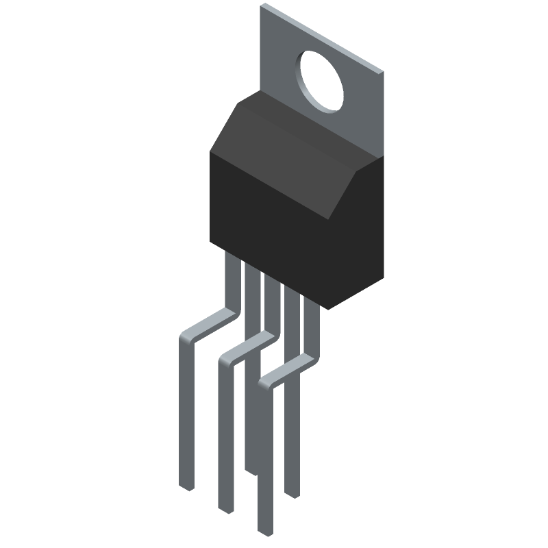 TDA2040V datasheet
by STMicroelectronics
TDA2040V datasheet
by STMicroelectronics
 Findchips
 Findchips