A good PCB layout for optimal thermal performance involves placing the device near a thermal pad or heat sink, using thermal vias to dissipate heat, and keeping the surrounding area clear of other components.
To ensure EMC, use a shielded enclosure, keep the device away from high-frequency sources, and use filtering or shielding on input/output lines. Also, follow the recommended PCB layout and grounding scheme.
Exceeding the maximum Tj rating can lead to reduced lifespan, decreased performance, and even permanent damage to the device. Ensure proper thermal management and heat dissipation to stay within the recommended operating temperature range.
Yes, the TDA1013B/N2,112 is suitable for high-reliability and automotive applications. However, ensure you follow the recommended operating conditions, and consider additional testing and validation for specific industry requirements.
To troubleshoot issues, start by reviewing the datasheet and application notes, checking the PCB layout and component placement, and verifying the power supply and input/output connections. Use oscilloscopes or logic analyzers to debug the issue, and consult NXP Semiconductors' support resources or a qualified engineer if needed.
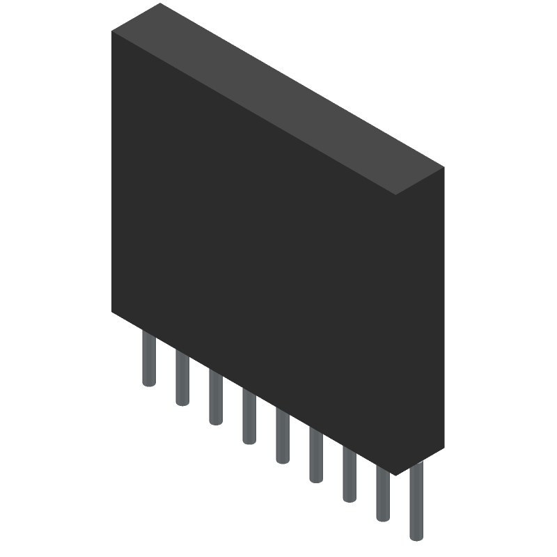 TDA1013B/N2,112 datasheet
by NXP Semiconductors
TDA1013B/N2,112 datasheet
by NXP Semiconductors
 Findchips
