STMicroelectronics recommends a thermal pad on the bottom of the package, connected to a large copper area on the PCB to dissipate heat efficiently.
Use a thermal management strategy, such as heat sinks or thermal interfaces, to keep the junction temperature below 150°C. Also, ensure proper PCB design and layout to minimize thermal resistance.
STMicroelectronics recommends using ESD protection devices, such as TVS diodes, on the input lines to protect the device from electrostatic discharge. Follow the IEC 61000-4-2 standard for ESD testing.
Use a 4-layer PCB with a solid ground plane, and keep the signal traces short and direct. Avoid vias and right-angle bends, and use a consistent impedance throughout the signal path.
Follow the JEDEC J-STD-020 standard for reflow soldering, with a peak temperature of 260°C and a dwell time of 30-60 seconds. Use a solder paste with a melting point above 217°C.
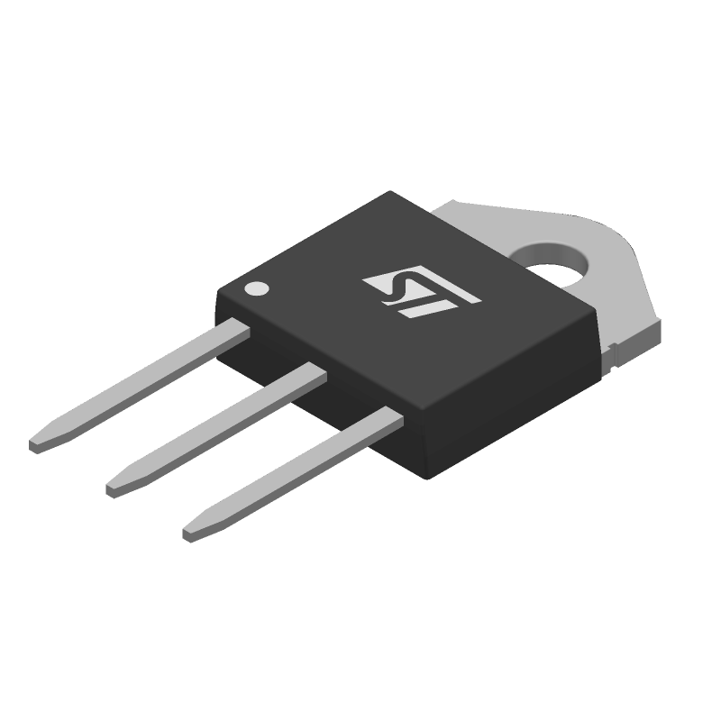 T1235T-8T datasheet
by STMicroelectronics
T1235T-8T datasheet
by STMicroelectronics
 Findchips
 Findchips