STMicroelectronics provides a recommended PCB layout in their application note AN5046, which includes guidelines for thermal pad connection, copper pouring, and via placement to ensure optimal thermal performance.
The thermal shutdown feature is enabled by default. To handle it, monitor the TSD (Thermal Shutdown) pin, which goes low when the junction temperature exceeds 170°C. When TSD is low, the device is in thermal shutdown mode, and the output voltage is disabled. Wait for the device to cool down before re-enabling the output voltage.
Although the datasheet specifies a maximum input voltage of 18V, it's recommended to limit the input voltage to 15V to ensure reliable operation and prevent damage to the internal components.
The output voltage ripple can be calculated using the formula: ΔVout = (Iout * ESL) / (Cout * fsw), where ESL is the equivalent series inductance of the output capacitor, Cout is the output capacitance, and fsw is the switching frequency. A lower ESL and higher Cout value can help reduce the output voltage ripple.
STMicroelectronics recommends using a low-ESR ceramic capacitor (e.g., X7R or X5R) with a value of 10uF to 22uF, depending on the input voltage and current requirements. This helps to filter out high-frequency noise and ensure stable operation.
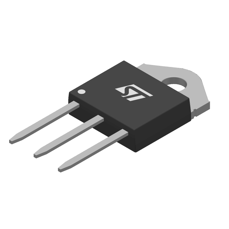 T1235H-8I datasheet
by STMicroelectronics
T1235H-8I datasheet
by STMicroelectronics
 Findchips
 Findchips