A good PCB layout for optimal thermal performance involves placing the device near a thermal pad or a heat sink, using thick copper traces for heat dissipation, and minimizing the distance between the device and the thermal pad or heat sink.
To ensure reliable operation at high temperatures, ensure that the device is operated within the recommended temperature range, use a suitable thermal interface material, and provide adequate heat sinking and airflow.
To prevent ESD damage, handle the device in an ESD-protected environment, use ESD-protective packaging and handling materials, and ensure that all personnel handling the device are grounded.
To troubleshoot issues with the device, check the PCB layout and thermal design, verify that the device is operated within the recommended specifications, and use diagnostic tools such as oscilloscopes and thermal imaging cameras to identify the root cause of the issue.
The recommended soldering and assembly techniques for the device involve using a soldering iron with a temperature range of 250-260°C, using a solder with a melting point of 217-220°C, and following the recommended assembly procedures outlined in the datasheet.
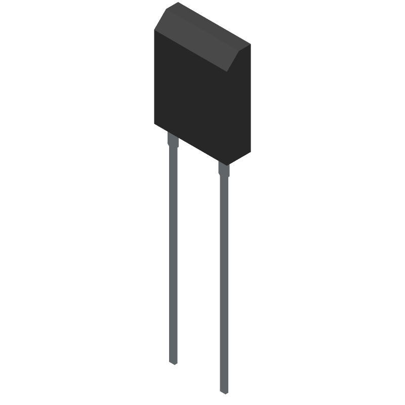 STTH6010WY datasheet
by STMicroelectronics
STTH6010WY datasheet
by STMicroelectronics
 Findchips
