A 2-layer or 4-layer PCB with a thermal relief pattern and a solid ground plane is recommended for optimal thermal performance. The thermal pad should be connected to the ground plane through multiple vias.
Ensure that the device is operated within the recommended junction temperature range (TJ) of -40°C to 150°C. Implement proper thermal management, such as heat sinks or thermal interfaces, to maintain a safe junction temperature.
A gate drive circuit with a high current capability (e.g., 1A to 2A) and a fast rise time (e.g., <10ns) is recommended. A gate resistor value between 10Ω to 22Ω is suitable for most applications.
Implement overvoltage protection (OVP) and overcurrent protection (OCP) circuits to prevent damage from voltage spikes and excessive current. A fuse or a current-sensing resistor can be used for OCP.
A dead time of 100ns to 200ns is recommended to prevent shoot-through currents and ensure reliable operation. The exact dead time value depends on the specific application and switching frequency.
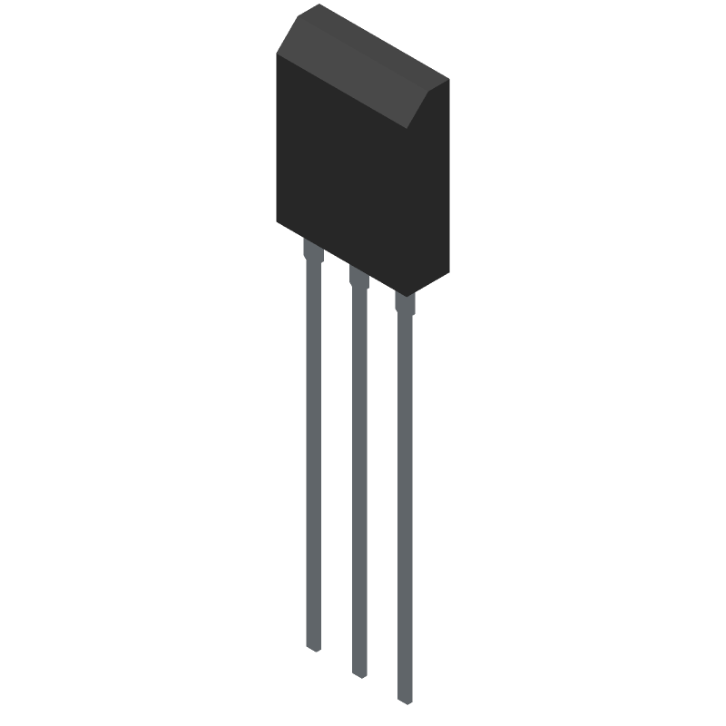 STPSC20H065CWY datasheet
by STMicroelectronics
STPSC20H065CWY datasheet
by STMicroelectronics