A good PCB layout for optimal thermal performance involves placing the device near a thermal pad or a heat sink, and ensuring good thermal conductivity between the device and the PCB. A 2-layer or 4-layer PCB with a solid ground plane is recommended. Avoid placing thermal vias under the device, and ensure that the PCB is designed to minimize thermal resistance.
To ensure reliable operation at high temperatures, ensure that the device is operated within the recommended temperature range (up to 150°C for the STPS1150AY). Use a suitable thermal interface material (TIM) between the device and the heat sink, and ensure good airflow around the device. Monitor the device's junction temperature and adjust the thermal design accordingly.
The recommended soldering conditions for the STPS1150AY are: peak temperature of 260°C, soldering time of 10-30 seconds, and a temperature ramp-up rate of 3°C/second. Ensure that the soldering process is lead-free and RoHS-compliant.
To handle the device's power dissipation, ensure that the PCB is designed to dissipate heat efficiently. Use a heat sink or thermal pad, and ensure good airflow around the device. Monitor the device's junction temperature and adjust the thermal design accordingly. Consider using a thermal interface material (TIM) to improve heat transfer between the device and the heat sink.
The STPS1150AY has built-in ESD protection, but it's still important to follow proper ESD handling procedures during assembly and testing. Ensure that the device is handled in an ESD-protected environment, and use ESD-protective packaging and materials.
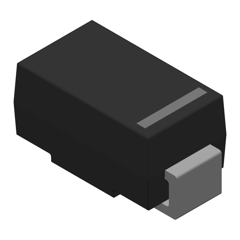 STPS1150AY datasheet
by STMicroelectronics
STPS1150AY datasheet
by STMicroelectronics
 Findchips
