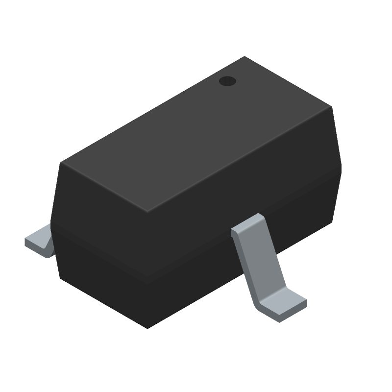
The recommended PCB footprint for SDMP0340LCT-7-F is a standard SOT23-6L package with a 1.8mm x 1.35mm body size. The datasheet provides a recommended land pattern and soldering guidelines.
To ensure output voltage stability, it's essential to follow the recommended capacitor values and placement guidelines in the datasheet. Additionally, consider the input voltage range, output current, and PCB layout to minimize noise and ripple.
The maximum input voltage for SDMP0340LCT-7-F is 6.5V. Exceeding this voltage may damage the device. Ensure your design stays within the recommended input voltage range to ensure reliable operation.
SDMP0340LCT-7-F is rated for operation up to 125°C. However, it's essential to consider the device's power dissipation, thermal resistance, and PCB design to ensure reliable operation in high-temperature environments.
To calculate power dissipation, consider the input voltage, output voltage, output current, and quiescent current. Use the datasheet's equations and graphs to estimate the power dissipation and ensure your design stays within the recommended operating conditions.
 SDMP0340LCT-7-F datasheet
by Diodes Incorporated
SDMP0340LCT-7-F datasheet
by Diodes Incorporated
 Findchips
