The recommended PCB footprint for the S3J-13-F is a standard SOT23-3 package with a 1.3mm x 1.3mm body size. A minimum pad size of 0.8mm x 0.8mm is recommended for reliable soldering.
To ensure proper biasing, connect the input pin (pin 1) to a voltage source through a resistor (e.g., 1kΩ) and a capacitor (e.g., 10nF) in series. This helps to filter out noise and ensure a stable input voltage.
The S3J-13-F is rated for operation from -40°C to 125°C. However, it's recommended to derate the device's performance at temperatures above 85°C to ensure reliable operation.
Yes, the S3J-13-F is AEC-Q100 qualified, making it suitable for automotive and high-reliability applications. However, it's essential to follow the recommended operating conditions and design guidelines to ensure the device meets the required reliability standards.
To prevent electrostatic discharge (ESD) damage, handle the S3J-13-F by the body or pins, avoid touching the die, and use an ESD wrist strap or mat when handling the device. Follow standard ESD handling procedures to prevent damage.
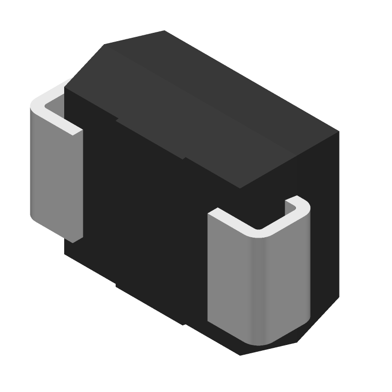 S3J-13-F datasheet
by Diodes Incorporated
S3J-13-F datasheet
by Diodes Incorporated
 Findchips
 Findchips