STMicroelectronics recommends a 2-layer PCB with a thermal pad connected to a large copper area on the bottom layer to dissipate heat efficiently.
Ensure proper heat sinking, use a thermally conductive interface material, and follow the recommended PCB layout guidelines. Also, consider derating the device's current handling capability at high temperatures.
Exceeding the maximum Tj rating can lead to reduced lifespan, increased thermal resistance, and potentially catastrophic failure. Always ensure the device operates within the recommended temperature range.
Yes, but be aware of the device's switching losses and ensure proper snubber circuits are implemented to minimize electromagnetic interference (EMI) and voltage spikes.
Implement proper EOS and ESD protection measures, such as TVS diodes, resistors, and capacitors, and follow proper handling and storage procedures to prevent damage.
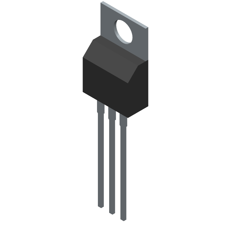 FERD40H100STS datasheet
by STMicroelectronics
FERD40H100STS datasheet
by STMicroelectronics