A 2-layer or 4-layer PCB with a thermal relief pattern and a solid ground plane is recommended. Ensure a minimum of 1 oz copper thickness and a thermal via array under the device.
Implement a robust thermal management system, including a heat sink, thermal interface material, and a cooling fan if necessary. Monitor junction temperature and adjust the system design accordingly.
Monitor the device's junction temperature, drain-source voltage, and drain current. Implement over-temperature, over-voltage, and over-current protection mechanisms to prevent damage.
Yes, but ensure the device is properly snubbed to minimize ringing and electromagnetic interference (EMI). Use a suitable gate driver and layout to minimize parasitic inductance and capacitance.
Choose a gate driver with a suitable output current capability, rise and fall times, and voltage rating. Ensure the driver can provide a high enough voltage to fully enhance the device, and consider using a dedicated gate driver IC or a discrete solution.
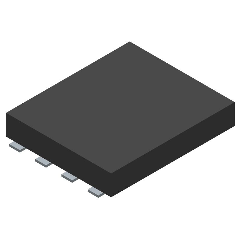 FERD20U60DJFD-TR datasheet
by STMicroelectronics
FERD20U60DJFD-TR datasheet
by STMicroelectronics
 Findchips
