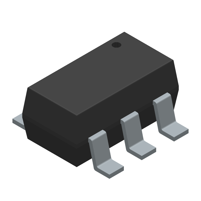
The recommended PCB footprint for the DMMT5551S-7-F is a standard SOT23 package with a 1.3mm x 1.3mm body size. A minimum pad size of 0.6mm x 0.6mm is recommended for reliable soldering.
To ensure proper biasing, connect the anode (A) to a voltage source (e.g., VCC) and the cathode (K) to ground through a current-limiting resistor. The recommended bias voltage is between 1.9V and 5.5V.
The maximum allowable power dissipation for the DMMT5551S-7-F is 250mW. Ensure that the device is properly heat-sinked and operated within the recommended temperature range to prevent overheating.
While the DMMT5551S-7-F is primarily designed for low-frequency applications, it can be used in high-frequency applications up to 100MHz. However, the device's performance may degrade at higher frequencies due to internal capacitance and inductance.
To prevent electrostatic discharge (ESD) damage, handle the DMMT5551S-7-F with an ESD wrist strap or mat, and ensure that the device is stored in an ESD-protected environment. The device has an internal ESD protection diode, but external protection measures are still recommended.
 DMMT5551S-7-F datasheet
by Diodes Incorporated
DMMT5551S-7-F datasheet
by Diodes Incorporated