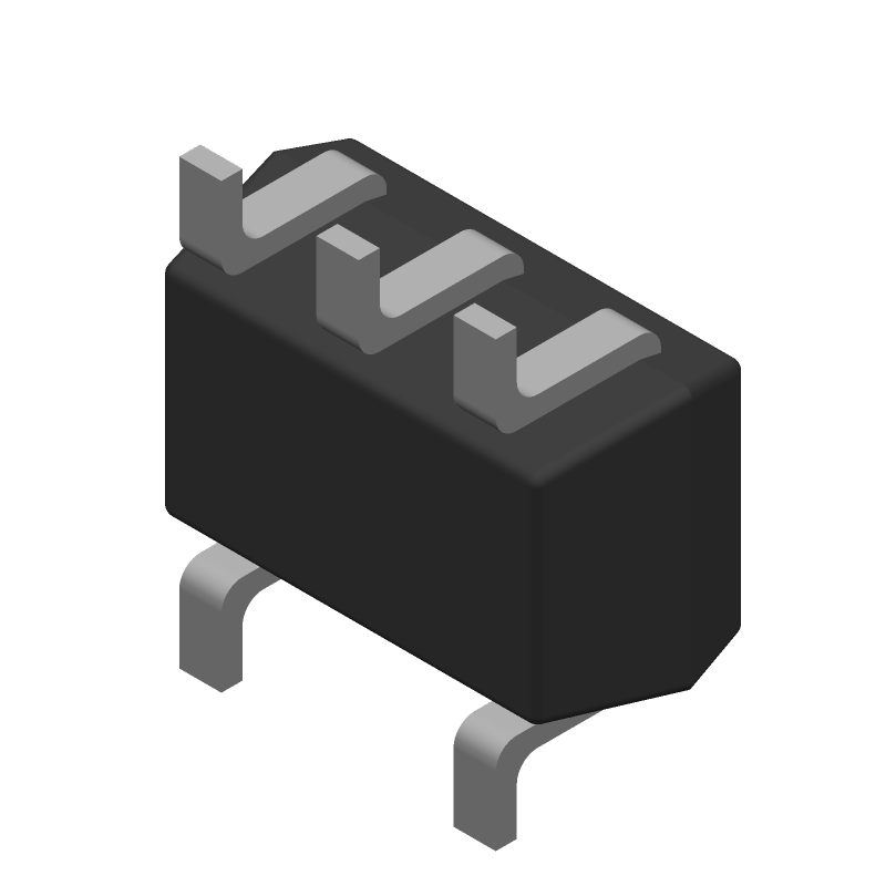
The recommended PCB footprint for the D1213A-02S-7 is a standard SOT23-6 package with a 1.3mm x 1.3mm body size. A minimum pad size of 0.8mm x 0.8mm is recommended for reliable soldering.
To ensure proper biasing, connect the input pin (VIN) to a stable voltage source between 2.5V to 5.5V, and the enable pin (EN) to a logic-level signal (0V or VIN). The output pin (VOUT) should be decoupled with a 1uF ceramic capacitor to ensure stability.
The D1213A-02S-7 is capable of delivering up to 1A of output current. However, it's recommended to limit the output current to 0.5A for optimal performance and to prevent overheating.
To ensure reliable operation, it's essential to provide adequate thermal management. A thermal pad on the PCB can help dissipate heat. Additionally, ensure good airflow around the device, and consider using a heat sink if the device is expected to operate at high temperatures or with high output currents.
While the D1213A-02S-7 is a general-purpose LDO regulator, it's not specifically designed for automotive applications. For automotive applications, consider using a dedicated automotive-grade LDO regulator that meets the required AEC-Q100 standards.
 D1213A-02S-7 datasheet
by Diodes Incorporated
D1213A-02S-7 datasheet
by Diodes Incorporated