The recommended land pattern for the BZT52C2V4S-7-F is a rectangular pad with a size of 0.8mm x 1.2mm, with a solder mask clearance of 0.1mm.
To handle the ESD sensitivity of the BZT52C2V4S-7-F, it is recommended to use ESD protection devices, such as TVS diodes, and follow proper handling and storage procedures to prevent ESD damage.
The maximum operating temperature range for the BZT52C2V4S-7-F is -40°C to 150°C, but it's recommended to operate within -40°C to 125°C for optimal performance and reliability.
Yes, the BZT52C2V4S-7-F can be used in high-frequency applications up to 1 GHz, but it's recommended to evaluate the device's performance in the specific application and consider the effects of parasitic inductance and capacitance.
To ensure the reliability of the BZT52C2V4S-7-F in a high-reliability application, it's recommended to follow proper design and manufacturing guidelines, including using a robust PCB design, selecting high-quality components, and implementing thorough testing and inspection procedures.
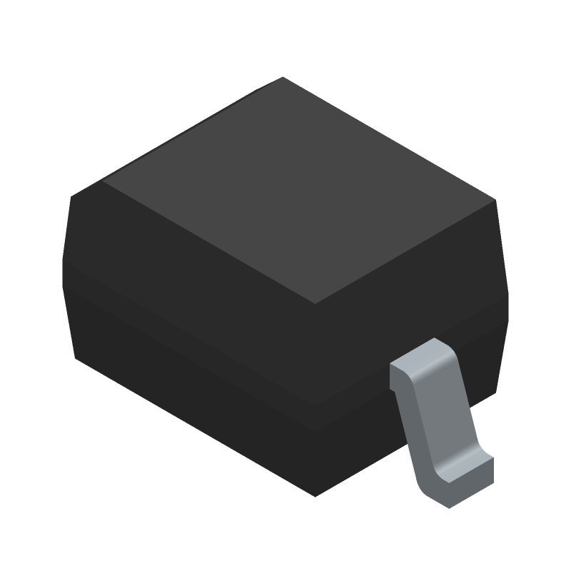 BZT52C2V4S-7-F datasheet
by Diodes Incorporated
BZT52C2V4S-7-F datasheet
by Diodes Incorporated
 Findchips
 Findchips