STMicroelectronics recommends a PCB layout with a large copper area connected to the drain pin (pin 3) to dissipate heat efficiently. A minimum of 2 oz copper thickness is recommended, and the copper area should be connected to a heat sink or a metal plate for better heat dissipation.
To ensure proper biasing, the gate-source voltage (Vgs) should be between 2V and 5V, and the drain-source voltage (Vds) should be between 10V and 400V. The recommended biasing circuit includes a voltage regulator, resistors, and capacitors to stabilize the voltage and reduce noise.
To prevent ESD damage, handle the device in an ESD-protected environment, wear an ESD wrist strap or use an ESD mat, and avoid touching the device's pins or leads. Use an anti-static bag or wrap the device in anti-static material during storage and transportation.
The gate resistor value depends on the specific application and the required switching frequency. A general guideline is to use a gate resistor between 1 kΩ and 10 kΩ. A higher value reduces the switching speed but increases the noise immunity, while a lower value increases the switching speed but reduces the noise immunity.
For high-power applications, ensure good thermal contact between the device and the heat sink or metal plate. Use a thermal interface material (TIM) to fill any gaps between the device and the heat sink. The heat sink should be designed to dissipate heat efficiently, and the system should be designed to minimize thermal resistance.
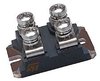 BYT200PIV-400 datasheet
by STMicroelectronics
BYT200PIV-400 datasheet
by STMicroelectronics
 Findchips
 Findchips