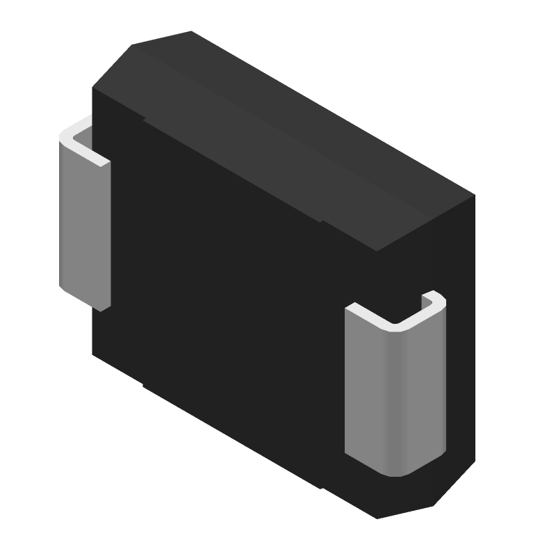
The recommended PCB footprint for the B320-13-F is a standard SOT23 package with a 1.3mm x 1.3mm body size. A minimum pad size of 0.8mm x 0.8mm is recommended for reliable soldering.
To ensure reliable operation in high-temperature environments, it is recommended to derate the maximum junction temperature (Tj) by 1°C for every 1W of power dissipation above 25°C. Additionally, ensure good thermal design and heat sinking to minimize thermal resistance.
The maximum allowable voltage for the B320-13-F is 20V. Exceeding this voltage may result in device damage or failure.
To prevent electrostatic discharge (ESD) damage, handle the B320-13-F with anti-static wrist straps, mats, or other ESD protection devices. Ensure that the PCB and assembly process also follow ESD-safe practices.
Store the B320-13-F in a dry, cool place with a temperature range of -40°C to 125°C. Avoid exposing the device to moisture, direct sunlight, or extreme temperatures.
 B320-13-F datasheet
by Diodes Incorporated
B320-13-F datasheet
by Diodes Incorporated