A good PCB layout for the ACPL-217-56CE involves keeping the input and output circuits separate, using a ground plane, and minimizing the length of the signal traces. It's also recommended to use a 4-layer PCB with a dedicated power plane and a dedicated ground plane.
To ensure reliability in high-temperature applications, it's essential to follow proper thermal management practices, such as providing adequate heat sinking, using a thermally conductive material for the PCB, and ensuring good airflow around the device.
The maximum allowable voltage for the ACPL-217-56CE is 560V, as specified in the datasheet. Exceeding this voltage can damage the device.
To troubleshoot issues with the ACPL-217-56CE, start by checking the power supply voltage, ensuring it's within the recommended range. Then, verify the input and output signals using an oscilloscope. If the issue persists, check the PCB layout and ensure it meets the recommended layout guidelines.
Yes, the ACPL-217-56CE is suitable for high-frequency applications up to 100 kHz. However, it's essential to follow proper PCB layout and design practices to minimize signal attenuation and ensure reliable operation.
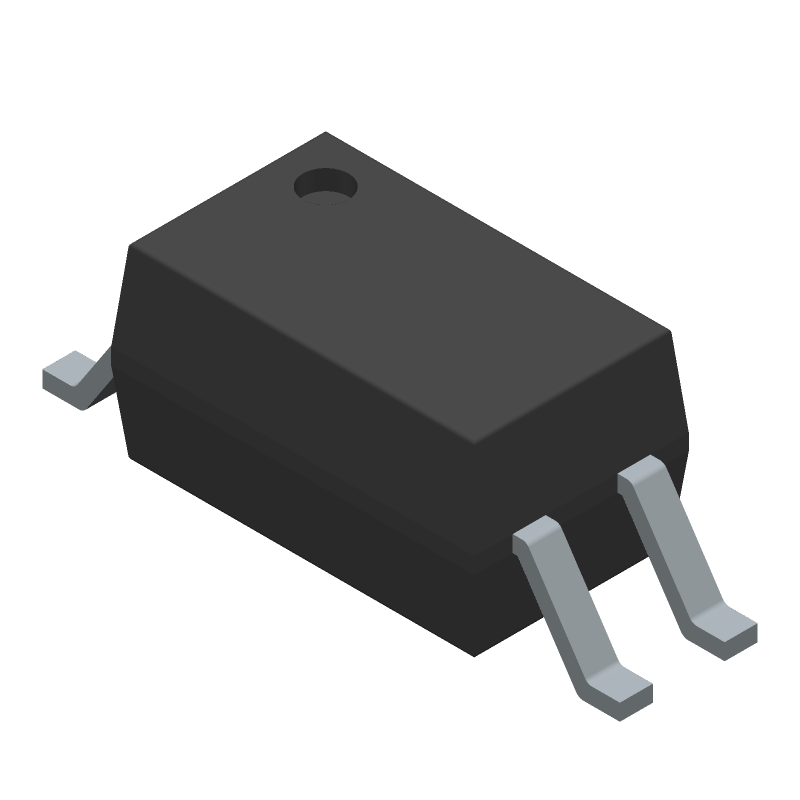 ACPL-217-56CE datasheet
by Avago Technologies
ACPL-217-56CE datasheet
by Avago Technologies
 Findchips
