The maximum safe operating area (SOA) for the 2N4033 is not explicitly stated in the datasheet, but it can be estimated based on the device's thermal and electrical characteristics. As a general rule, it's recommended to operate the device within the specified maximum ratings and avoid operating conditions that may cause excessive heat, voltage, or current stress.
To ensure the 2N4033 is properly biased for linear operation, you should follow the recommended biasing conditions outlined in the datasheet. This typically involves setting the base-emitter voltage (VBE) and collector-emitter voltage (VCE) within the specified ranges, and ensuring the device is operated within the recommended current and power dissipation limits.
The recommended PCB layout and thermal management for the 2N4033 involve following good design practices for high-power transistors. This includes using a thermally conductive PCB material, providing adequate heat sinking and thermal relief, and minimizing thermal resistance between the device and the heat sink. Additionally, it's recommended to follow the manufacturer's guidelines for PCB layout and thermal management.
Yes, the 2N4033 can be used as a switch, but it's essential to ensure the device is operated within its recommended switching frequency range. The datasheet typically provides guidance on the maximum switching frequency, and it's recommended to follow these guidelines to avoid excessive power dissipation, electromagnetic interference (EMI), and other issues.
To protect the 2N4033 from electrostatic discharge (ESD), it's recommended to follow standard ESD protection practices, such as using ESD-safe handling and storage procedures, implementing ESD protection circuits, and ensuring the device is properly grounded during handling and assembly.
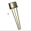 2N4033 datasheet
by STMicroelectronics
2N4033 datasheet
by STMicroelectronics